In the previous post on Ideal IV characteristics of MOSFET, we derived the current-voltage relationship assuming a certain number of ideal conditions. But in practical scenarios, there are a lot of non-ideal effects that one needs to keep in mind. In this post, let’s try to get hold of the physical phenomena that cause the non-ideal IV characteristics of a MOSFET.
We will also get some idea behind the working of the MOS capacitor for a better understanding of the inversion layer formation. This will also give us an idea of gate capacitance which limits certain functionalities of the MOSFET.
So before we begin, make sure you find yourself comfortable with the ideal working of a MOSFET and the current-voltage relationships obtained in the previous post of this CMOS course. If not, now will be an excellent time to head back to the last post and revise the derivations and the results obtained in the ideal case.
Contents
Short Channel Effects
Most of the non-ideal effects we will discuss in this post are due to what is commonly regarded as “Short Channel Effects”.
Generally, in order to improve the performance and reduce the cost of production, one would prefer to scale down the size of the transistors. This scaling down also eliminates many stray capacitances that are present in the overall device. Ultimately increasing the speed of operation.
But when the channel length is scaled down to the order of the depletion layer, a certain number of non-ideal effects come into play. These second-order effects will be the main focus of this post.
Channel Length Modulation
As we keep on increasing our 

Some of us might be familiar with a similar effect in the case of BJT known as “Base Width Modulation“. Thus we get a 
Generally, the fabrication of the MOSFET devices is done in a way such that the change in length given by 

Model for channel length modulation
To model the channel length modulation, we use the following constructs:
 ; here
  is a parameter that is used to quantify the channel length modulation effect. We always aim at keeping the as small as possible.
Solving, we get 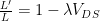

Hence, 
Inserting the above result in the current equation for saturation mode we get:
![I_{D} = \frac{\mu_{n} W C_{ox}}{2 L} [(V_{GS} - V_{T})^2] (1 + \lambda V_{DS})](https://s0.wp.com/latex.php?latex=I_%7BD%7D+%3D+%5Cfrac%7B%5Cmu_%7Bn%7D+W+C_%7Box%7D%7D%7B2+L%7D+%5B%28V_%7BGS%7D+-+V_%7BT%7D%29%5E2%5D+%281+%2B+%5Clambda+V_%7BDS%7D%29+&bg=ffffff&fg=000&s=0&c=20201002) .
.
Hence from the equation one can see the relation of
In the plot of figure 2, we can see the effect of Channel Length Modulation, here even when 
Ideally, we would want the current to saturate up once the drain-to-source voltage exceeds the overdrive voltage. Hence the least the variation of current in the saturation region the better is the quality of transistor operation. The parameter
Early Voltage

Suppose we take the different IV curves in their saturation region and extrapolate them towards the negative axis for 


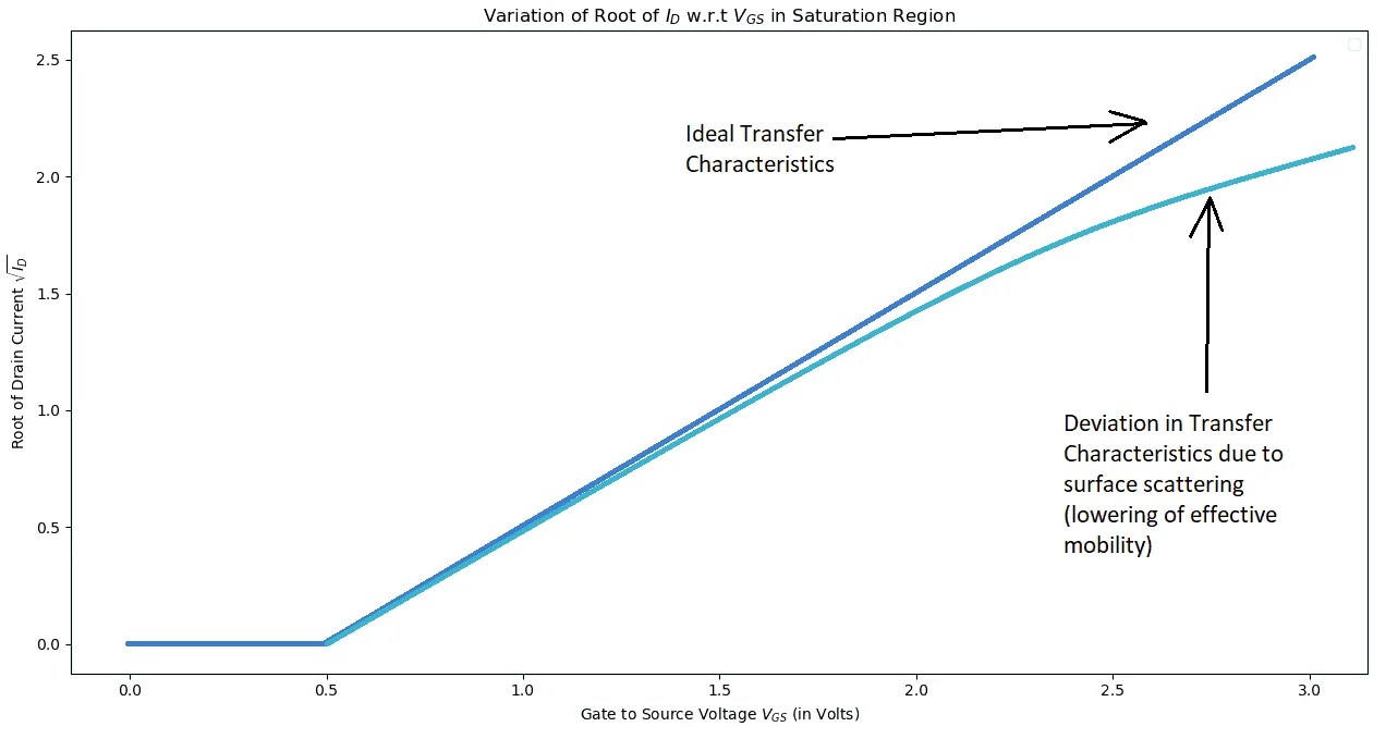
Mobility Degradation (Surface Scattering)
Practically, the electrons traveling from the source to drain in an NMOS don’t follow a straight path. For most cases, the lateral electric field is much more than the vertical electric field. But still, there is some non-zero vertical electric field present in the inversion channel.

Suppose an electron is starting from the source terminal edge, as shown in figure 4. This electron will be under the influence of both the electric fields. Thus it will move towards the drain and also will be attracted towards the oxide layer (Keep in mind that the pull towards the oxide layer will be very low). As the electron gets very close to the practically uneven oxide interface, it will be scattered and follow a path towards the downward direction. Again this electron will be attracted by the electric field, and the process continues. Thus trajectory for the electron will be more of a zig-zag one rather than a linear one.
This effect will only be dominant for the electrons that are closer to the oxide interface. As the vertical electric field is weaker, most of the electrons which start far away from the oxide interface will reach the drain before they encounter a scattering event. But as we scale down the size of the transistor, more fraction of electrons will be scattered as more fraction of electrons will be in close proximity of the oxide layer.
So the effective path traveled by the electrons in the inversion layer will be higher in the case of transistors with small size. Hence this can be modelled with an effective decrease in the mobility of electrons.
Effective mobility of electrons can be given by the empirical formula as:
 .
.
Here 


Velocity Saturation
Recall that while deriving the ideal characteristics for NMOS, we took the drift velocity of the electrons in the inversion layer to be proportional to the lateral electric field applied. The proportionality constant was given by 
The exact formula for the drift velocity can be given as:

The term 


If we solve for the drain current by considering the above stated value of drift velocity, we get:
![I_{D} = \frac{\mu_{n} W C_{ox}}{2 L}[2 (V_{GS} - V_{T}) V_{DS} - V^{2}_{DS}] [\frac{1}{1 + V_{DS}/(E_{C}L)}]](https://s0.wp.com/latex.php?latex=I_%7BD%7D+%3D+%5Cfrac%7B%5Cmu_%7Bn%7D+W+C_%7Box%7D%7D%7B2+L%7D%5B2+%28V_%7BGS%7D+-+V_%7BT%7D%29+V_%7BDS%7D+-+V%5E%7B2%7D_%7BDS%7D%5D+%5B%5Cfrac%7B1%7D%7B1+%2B+V_%7BDS%7D%2F%28E_%7BC%7DL%29%7D%5D&bg=ffffff&fg=000&s=0&c=20201002)
This is exactly our previous formula for the current multiplier with an additional term referred to as 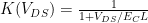
Now as we keep on increasing the 

Suppose this value of 
![I_{D} = \frac{\mu_{n} W C_{ox}}{2 L}[2 (V_{GS} - V_{T}) V_{Dsat} - V^{2}_{Dsat}] K(V_{Dsat})](https://s0.wp.com/latex.php?latex=I_%7BD%7D+%3D+%5Cfrac%7B%5Cmu_%7Bn%7D+W+C_%7Box%7D%7D%7B2+L%7D%5B2+%28V_%7BGS%7D+-+V_%7BT%7D%29+V_%7BDsat%7D+-+V%5E%7B2%7D_%7BDsat%7D%5D+K%28V_%7BDsat%7D%29+&bg=ffffff&fg=000&s=0&c=20201002)
Body Effect (Back Gate Effect)
Recall that in our previous derivation for the ideal IV characteristics, the biasing scheme we used had the source and the body both connected to ground. But in practical design applications, one might not be left with a choice to connect the source to the ground.
For example, the NMOS we are using might be a cascading stage whose source is connected to another MOSFET. In such scenarios, the difference in potential between the body and the source terminal causes a change in the threshold voltage of the MOSFET. This effect of change in threshold voltage is called the “Body Effect” or the “Back Gate Effect”.
Physical Process
In this part, we will try to get an intuitive understanding of the physical phenomenon that causes the body effect.

Suppose we use the above biasing scheme, hence there is a non-zero 
From the MOS capacitor equations, one can understand that the threshold voltage of the MOS is also proportional to the density of electrons in the depletion layer.
Hence as we accumulate more and more electrons in the depletion layer below the oxide interface, there will be an increase in the value of threshold voltage. One can also understand this by the fact that the gate being metal will try to mirror the magnitude of charge that is present on the other side of the oxide (dielectric). Hence we will need more charges and thus more gate voltage in order to get the transistor out of cut-off.
Mathematical Formulae
The expression we obtain for threshold voltage from the MOS capacitor physics can be used to obtain the change in the threshold voltage due to body effect. The change in threshold voltage is given by:
![\Delta V_{T} = \gamma [\sqrt{\phi_{s}} - \sqrt{2 \phi_{f}}]](https://s0.wp.com/latex.php?latex=+%5CDelta+V_%7BT%7D+%3D+%5Cgamma+%5B%5Csqrt%7B%5Cphi_%7Bs%7D%7D+-+%5Csqrt%7B2+%5Cphi_%7Bf%7D%7D%5D+&bg=ffffff&fg=000&s=0&c=20201002)
Here the 


The factor 

Hence our final equation for the threshold voltage becomes:
![V_{Tb} = V_{To} + \gamma [\sqrt{2 \phi_{f} + V_{SB}} - \sqrt{2 \phi_{f}}]](https://s0.wp.com/latex.php?latex=+V_%7BTb%7D+%3D+V_%7BTo%7D+%2B+%5Cgamma+%5B%5Csqrt%7B2+%5Cphi_%7Bf%7D+%2B+V_%7BSB%7D%7D+-+%5Csqrt%7B2+%5Cphi_%7Bf%7D%7D%5D+&bg=ffffff&fg=000&s=0&c=20201002)
For a typical MOSFET, we have the body bias coefficient = 

Drain Induced Barrier Lowering(DIBL)
Recall that for the electron conduction to happen we apply a positive drain-to-source potential. The

As we increase our 
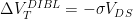
The fitting parameter \signa is also dependant on the length of the MOSFET channel. With an increase in channel length L, the value of 
Leakage Current Effects
There are certain non-ideal effects that result in leakage of some undesired currents in the MOSFET. We can have non-zero values of current through the different terminals of the MOSFET even when we ideally expect them to be zero. These non-ideal effects are important in estimating the power consumed or the energy efficiency of the circuit composed of a large number of transistors. The cross-sectional view of the transistor in the diagram of figure 10 shows the different current leakage effects that are present in an NMOS transistor.

Subthreshold Conduction
Previously we have discussed that for the conduction to happen in the MOSFET; we need the 

From experimental results, one can observe that there is still some non-zero current flowing from drain to source even when we are operating at a region with 


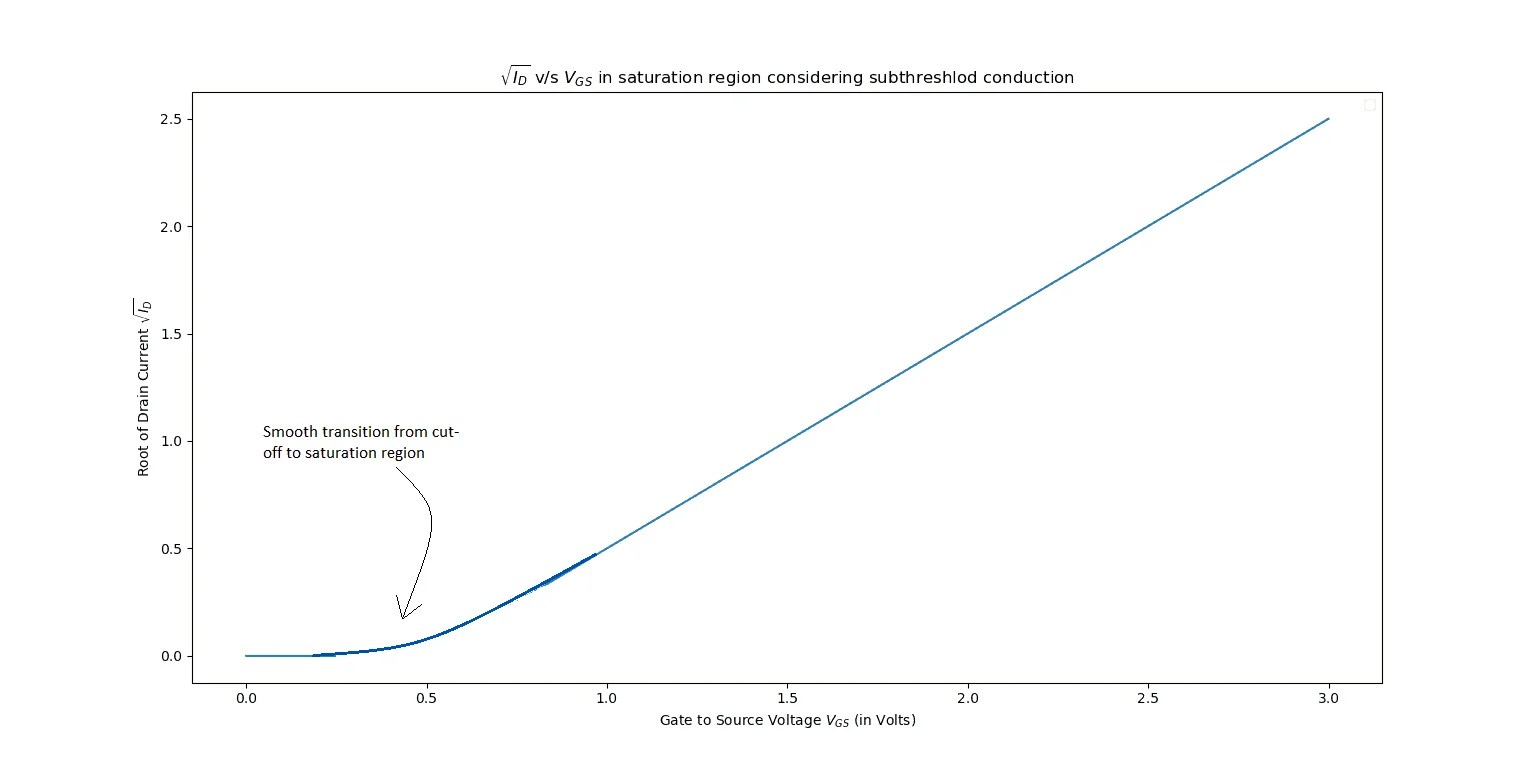
An empirical formula showing the relationship of current with
 ( 1 –
( 1 – )
)
Note that

Here the factor 
Gate Tunneling
Recall from the last post that in our ideal case, we assumed that the current going into the drain is equal to the current coming out of the source. As the oxide layer is an insulating material, there is no current that can flow into the channel from the gate terminal. This is indeed true for “large enough” oxide thickness.
However, generally, we would also like to reduce the thickness of the oxide layer in order to have a high capacitance per unit length. A high capacitance per unit length(
But there is a limit to which we can decrease our oxide thickness. Even for short channel devices as we keep on decreasing the size of our devices, we also need to shrink down the thickness of the oxide. Thus the probability of an electron tunneling through the oxide layer and entering the inversion channel increases. This limits the minimum thickness of the oxide layer we can use in practice. Practically, we can go till the oxide thickness is around 1.5 nm avoiding any tunneling phenomena.
The probability of tunneling is also inversely proportional to the dielectric constant of the medium(
Reverse Bias Diode Current (Junction Leakage)
In an NMOS transistor, the source and the drain are made up of n-type semiconductors. The substrate/body is made up of a p-type semiconductor.
If we assume the general biasing scheme, then both the source and the body are connected to the ground. But the potential applied at the drain terminal is positive w.r.t. the body. Thus we can see that the p-n junction formed by the body-drain junction is under reverse bias.
Previously we did not consider this effect because the reverse bias current magnitude (due to minority carriers) is much lower than the currents which are due to majority carriers.
The equation for the reverse bias current in a p-n junction is given by:

Here, 


 (the reverse sign shows the current is from drain to body)
In most of the cases, this current can be neglected with very little error introduced. But, if we have a relatively higher A (junction area) due to a large width (W), then this reverse bias current can cause a good amount of deviation.
MOS Capacitor
Until this point, we have not discussed the working of a MOS capacitor much. In this section, we will have a brief discussion of the working principle of the MOS capacitor.
We will see the results we can obtain about the capacitance-voltage relationship. The exact physics and the equations will not be discussed; rather, we will mainly focus on the models used. But if someone is really interested, it is suggested to go through some of the standard texts regarding semiconductor physics.
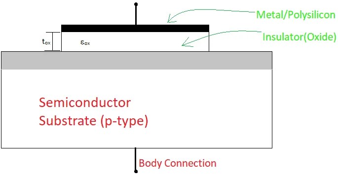
The diagram of figure 12 shows a cross-section of the MOS capacitor. It consists of a metal/polysilicon gate, an oxide layer, and a semiconductor substrate. We can observe that forming n-wells in the p-substrate on both sides of the oxide will give us the MOSFET structure. Here we will only concern ourselves with the working of a p-type MOS capacitor, i.e. the substrate is made up of p-type semiconductor. But the working of an n-type MOS capacitor will also be analogous.
Modes of operation
The energy band diagrams of a p-type MOS capacitor showing different applications of gate voltage is shown in figure 13.

As shown in the energy band diagrams, when we apply a negative gate voltage, then we are in the “Accumulation Mode”. The applied voltage attracts more holes toward the gate. In this mode of operation, the interface has more accumulated numbers of holes near the oxide interface than the bulk. Thus the semiconductor becomes more p-type near the interface than the bulk.
As we start increasing gate voltage, we enter the “Depletion Mode” when the gate voltage has a small positive value. Note that if we started off with materials such that the Fermi energy level of the metal was higher than that of the semiconductor, then even at zero gate voltage we will be in depletion mode. In this mode, there is a formation of an induced space charge region near the oxide interface, as shown in the diagram.
As we further increase the gate voltage, we will transit into “Inversion Mode”. As shown in the diagram, in this mode of operation, the Fermi energy level of the semiconductor is higher than it’s intrinsic Fermi level. This means that the semiconductor has turned into an n-type near the oxide interface.
Capacitance-Voltage(CV) characteristics
One can solve for the values of capacitance at the different modes discussed above. But here we will only be discussing the results we obtain after solving for the capacitance. We will also see how one can model the MOS capacitor for different modes of operation.
Accumulation Mode
In the accumulation mode, there are excess positive carriers in the semiconductor near the oxide interface. These charges can mirror the charges on the metal side and hence the overall system is equivalent to two parallel plates with a silicon-di-oxide sandwiched between them. So our capacitance in accumulation mode is:

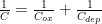
Depletion Mode
When we enter the depletion mode, we get a corresponding depletion capacitance which will be in series with the oxide capacitance. As we keep on increasing the gate voltage, the depletion width increases. Hence, our total capacitance also decreases with an increase in the gate voltage. This can be understood by the equations mentioned below:
Here, 

In the equation, 

Hence, we get 
Just before the onset of inversion, this capacitance reaches it’s minimum value as the depletion width is now maximum. This value of capacitance is called 
Inversion Mode
When we are in the inversion mode, there are two possible scenarios that can happen:
Low-frequency CV characteristics
If the input signal frequency is low, then the charges in the inversion layer get enough time to adjust themselves. Thus these charges can mirror the charges in the gate, and thus we will get a result similar to that obtained in the accumulation mode. This time the charges are electrons rather than the holes. So our capacitance will be:
 ; i.e. equal to the oxide capacitance.
High-frequency CV characteristics
For high-frequency input signals, the inversion charges don’t get enough time to exactly mirror up the charges in the gate. Rather they settle at an equilibrium constant value. So, effectively our capacitance will remain the same as it were in the case of depletion mode. Thus for voltages higher than the threshold voltage, we will have:


Finally, we obtained the CV characteristics of the MOS capacitor, as shown in figure 14. The CV characteristics for low-frequency signal and high-frequency signal differs only in the inversion mode of operation. In the inversion mode, the low-frequency curve is shown by dashed lines and the high-frequency curve is shown using solid lines.
Parasitic Components
Parasitic Capacitance in MOSFET
The MOSFET structure consists of various stray capacitances. These capacitances are a major factor that limits the speed of operation of transistors. Hence, while designing a circuit one needs to keep an account of these capacitances in order to predict the maximum frequency till which the circuit can function appropriately. We will only discuss the causes of some important parasitic capacitances present in the MOSFET. The physical location of these capacitances are illustrated in the diagram of figure 15.

Overlap Capacitance
Due to the fabrication process, there is a region of the oxide and gate layer that overlaps above the drain and the source n-wells. Thus we will have a metal layer and an n-type semiconductor separated by an oxide layer. This essentially acts as a parallel plate capacitance.
The more the area of overlap, the more will be the value of this parasitic capacitance. Thus to reduce the overlap capacitance, we will have to make sure that the area of overlap above the drain and the source region is as small as possible.
Junction Capacitance
Generally, when we design circuits using MOSFETs, we connect the body terminal of the NMOS device to the ground. The potential at the drain and the source terminal is positive w.r.t. the body terminal. Thus, the p-n junctions between the source-body and the drain-body is under reverse bias.
The reverse bias results in the formation of a depletion region. Hence, these also result in the formation of a reverse bias capacitance. This capacitance will increase as we increase the junction area between the p-type and the n-type regions.
Gate Capacitance
This is one of the most evident sources of parasitic capacitance for the MOSFET operation. As discussed in the MOS capacitor portion, the different modes result in the formation of different gate capacitances. The gate and the p-type body is separated by the oxide layer. This, in turn, also acts as a parallel plate capacitance.
The gate capacitance varies for different modes of operation. In accumulation mode, it is only due to the oxide layer capacitance. But if we enter into depletion mode, the induced depletion region thickness is also required to be taken into account. Also, in inversion mode, its value will change again.
Parasitic Resistance in MOSFET
Similarly, like the parasitic capacitances that are present in the circuit, there will be parasitic resistances. The parasitic resistances are also to be taken into account when are designing a certain analog or digital circuit. In many applications, it can limit the performance of the circuit and also increase power consumption. One of such major parasitic resistance present in the MOSFET structure is due to contact resistances.
Recall that the 3D structure used at the very start of the previous post contained metal contacts over the drain and source. These are called “Metal Contacts”, and they are used to connect the MOSFET terminals to the external circuits. In principle, the whole MOSFET operation is based on the fact that we control the resistance between the drain and source terminal by adjusting the gate voltage.

Now, suppose that the resistivity of the channel is 


Then, the effective resistance offered by the MOSFET between the source and the drain is then given by:

Here, 


This extra serial resistance
Conclusion
In this post, we have seen the different second-order effects present in a MOSFET. We have seen how these non-ideal scenarios affect our ideal IV characteristics. A special emphasis was given to Short Channel Effects. For some of the non-ideal effects, we have also gone through the mathematical expressions to get a better understanding. By the end of this post, we briefly covered the MOS capacitor characteristics and how the channel inversion layer is formed. Finally, we discussed some of the parasitic resistive and capacitive components present in the MOSFET structure. You need to be familiar with these effects while designing analog and digital circuits. These effects can degrade the performance of the circuits to a large extent.
In the next post, we will begin with the CMOS inverter design. We will go through the working of the CMOS inverter in detail. We will also discuss a certain number of parameters that are important for CMOS design.