In the modern world, we are surrounded by digital electronics all around us. Most of these digital electronics are made using semiconductor devices. One of the major breakthroughs in the field of electronics was the introduction of CMOS technology. The term CMOS stands for “Complementary Metal Oxide Semiconductor,” this means that we use both NMOS and PMOS devices in order to achieve the desired digital logic.
In this post and the ones that follow, we will go through the transistor level implementation of CMOS technology. We will try to understand how each of the gates are formed using simple transistor devices. As we are concerned with CMOS technology, we will only be dealing with logic gate implementations using MOSFETs. For the design of gates, the factors a designer must have in mind are as follows:
- Speed: What is the maximum delay caused by the circuit. What are the speed limits?
- Power: How much power is drawn by the circuit while operating at a certain speed?
- Noise: How much noise in the input signal can the circuit handle without degrading the output signal?
We will try to answer these questions as we move forward with this CMOS course. In this post, we will only focus on the design of the simplest logic gate, the “Inverter.” We will try to understand the working of the CMOS Inverter, its Voltage Transfer Characteristics, and an important parameter called “Noise Margins.”
The exact detailed physics of the MOSFET device is quite complex. But even if we consider the simple ideal current-voltage relationships, we can conclude a lot about the working of the CMOS inverter.
Hence, before we begin this post, make sure that you are comfortable with the IV relation in different modes of operation for both NMOS and PMOS devices (Ideal IV characteristics as well as Non-ideal IV characteristics). Additionally, at some point, we will be considering some concepts for channel length modulation i.e., how the current still varies with drain-to-source voltage in the saturation region.
Contents
Fundamental results on working of MOSFETs
In this section, we will discuss some of the results of a MOSFET, which will help us in the upcoming sections of the post. The results derived here assumes that the reader is aware of “Small Signal Analysis.” If that is not the case, then please go through some of the standard texts that discuss small-signal analysis in a generic manner.
Small signal gain(gm) of MOSFET
We have seen the drain current for an NMOS in the saturation region of operation, is given by:
![I_{D} = \frac{\mu_{n} W C_{ox}}{2 L} [(V_{GS} - V_{T})^2] (1 + \lambda V_{DS})](https://s0.wp.com/latex.php?latex=+I_%7BD%7D+%3D+%5Cfrac%7B%5Cmu_%7Bn%7D+W+C_%7Box%7D%7D%7B2+L%7D+%5B%28V_%7BGS%7D+-+V_%7BT%7D%29%5E2%5D+%281+%2B+%5Clambda+V_%7BDS%7D%29+&bg=ffffff&fg=000&s=0&c=20201002) .
.![I_{D} = \frac{k_{n}}{2 } [(V_{GS} - V_{T})^2] (1 + \lambda V_{DS})](https://s0.wp.com/latex.php?latex=+I_%7BD%7D+%3D+%5Cfrac%7Bk_%7Bn%7D%7D%7B2+%7D+%5B%28V_%7BGS%7D+-+V_%7BT%7D%29%5E2%5D+%281+%2B+%5Clambda+V_%7BDS%7D%29+&bg=ffffff&fg=000&s=0&c=20201002) .
.
Now, suppose we want to see how much the drain current changes with an infinitesimal change of the gate-to-source voltage. For this, we differentiate our drain current(


Here, the quantities 
As an approximate value, we can neglect the effect of channel length modulation, and then we get:

Some of the alternate forms of the equation are given by manipulating the current-voltage relations:
 =
=  .
.
 =
=  .
.
Thus, the simplest small-signal model of an NMOS device is shown in figure 1:

You can observe that we have placed a voltage-controlled current source between the drain and source terminal.
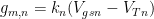
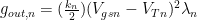
Output resistance of the MOSFET
The MOSFET in its saturation region can be thought of as an ideal current source. The current through the MOSFET doesn’t depend on the voltage across it, which is 
To take into account this effect, we find out the derivative of drain current
![\frac{d I_{D}}{d V_{DS}} = \frac{k_{n}}{2 } [(V_{GS} - V_{T})^2] (\lambda)](https://s0.wp.com/latex.php?latex=+%5Cfrac%7Bd+I_%7BD%7D%7D%7Bd+V_%7BDS%7D%7D+%3D+%5Cfrac%7Bk_%7Bn%7D%7D%7B2+%7D+%5B%28V_%7BGS%7D+-+V_%7BT%7D%29%5E2%5D+%28%5Clambda%29+&bg=ffffff&fg=000&s=0&c=20201002) .
.
Output conductance = ![g_{out} = \frac{k_{n}}{2 } [(V_{GS} - V_{T})^2] (\lambda)](https://s0.wp.com/latex.php?latex=+g_%7Bout%7D+%3D%C2%A0+%5Cfrac%7Bk_%7Bn%7D%7D%7B2+%7D+%5B%28V_%7BGS%7D+-+V_%7BT%7D%29%5E2%5D+%28%5Clambda%29+&bg=ffffff&fg=000&s=0&c=20201002)
Also we can approximate this to:

Taking the inverse of this derivative gives us the small-signal resistance that is present between the source and drain terminal.
![r_{o} = [\frac{d I_{D}}{d V_{DS}}]^{-1} = \frac{1}{\lambda I_{D}}](https://s0.wp.com/latex.php?latex=+r_%7Bo%7D+%3D+%5B%5Cfrac%7Bd+I_%7BD%7D%7D%7Bd+V_%7BDS%7D%7D%5D%5E%7B-1%7D+%3D+%5Cfrac%7B1%7D%7B%5Clambda+I_%7BD%7D%7D+&bg=ffffff&fg=000&s=0&c=20201002)

Thus, the final small-signal model we obtain for a MOSFET is shown in figure 2.
Differences in PMOS and NMOS
Low side and High side switch
Before we begin, there is a subtle point to note about the NMOS and PMOS transistors.
The source for the NMOS transistor is generally connected to the lowest potential w.r.t. the drain or the body. Thus, if we connect the drain of the transistor to some other arbitrary circuit, by controlling the gate potential, we can pull down the drain connection to ground when we enter into the saturation region. Hence, the NMOS transistors are generally used as “pull-down” or “low-side” switch.
On the contrary, the source of the PMOS is generally connected to the highest most potential w.r.t. the drain or the body. In a similar manner, the PMOS transistor can be used to pull up any circuit node to the highest potential (supply potential) in the circuit. Thus the PMOS transistors are generally used as “pull-up” or “high-side” switch.
Mobility Considerations
One more thing to note is that the electron mobility is almost twice as that of the hole mobility. Hence we have:
 ; keeping other parameters equal, we get:

Hence, if we have an NMOS and a PMOS of equal dimensions and both operating at the same voltages, then the current for the PMOS will be roughly half that of the NMOS. Moreover, the “on-conductance” of the PMOS will be half that of the NMOS.
In common practice, to obtain symmetrical operations in the circuit, the width (W) of the PMOS should be kept roughly twice of the NMOS. But due to some other non-ideal effects, it is not kept exactly to be twice. These will be discussed in detail once we start off with the formal derivations of input-output relation in a CMOS device.
Working of CMOS inverter
In this section, we will see in detail the construction of the CMOS inverter. We will see it’s input-output relationship for different regions of operation.
Circuit of a CMOS inverter
A detailed circuit diagram of a CMOS inverter is shown in figure 3. The different voltages are also marked in the diagram itself.

The body terminal of NMOS is connected to the ground (here denoted as 

 = gate-to-source voltage of NMOS =
  .
.
 = drain-to-source voltage of NMOS =
  .
.
 = gate-to-source voltage of PMOS = –
  .
.
 = drain-to-source voltage of PMOS =
  –
–  .
.
A simplified notation of the CMOS inverter circuit generally used is shown in figure 4.

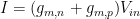
In this post, we will only be considering the static behavior of the inverter gate. This means that we don’t have any load resistance connected to the output terminal. The voltages are varying very slowly. Thus, the MOSFET parasitic capacitances can be neglected (open-circuited). This type of condition is called “Pseudo-Static.”
As there is no resistance, we can write: 
The current flowing from supply line 


Regions of operation
We divide the functioning of MOSFET over five regions of operation. These regions are discussed in detail below. For some of the cases, the calculations for the input-output relation become very lengthy. So, we will only discuss the equations and the method to obtain the final results. If interested, the readers can go through the calculations by themselves.
Operation Stage 1
Suppose we apply an input voltage such that:

Then, we are sure that the NMOS transistor M1 is in the cut-off region. Therefore, the crossover current will be zero at this point of operation. The potential at the output terminal is equal to the supply voltage
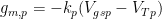
For the PMOS transistor M2, the source to gate voltage 

In the linear region, the conductivity of the PMOS transistor is given by:

On the other hand, the conductivity of NMOS transistor M1 is 0.
To summarise, 
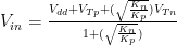
Operation Stage 2
As we keep on increasing the input voltage, we will cross the 
For PMOS transistor, the 

For NMOS, we can write:
 =
=  (Vin – VTn)2
And, for the PMOS, we can write:
 =
=  [2(Vin – Vdd – VTp)(Vout – Vdd) – (Vout – Vdd)2]
The quantity 

As there is no resistive load attached to the output terminal, we can equate both the currents:
 ; this gives us a quadratic in
  .
.
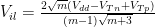
The final solution from solving the above equation is:
 = (Vin – VTp) +
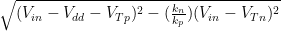
The overall equation is very complex, but for our understanding we will just have to make some simple observations. We can observe from the equation that as we increase 

Operation Stage 3
The previously mentioned voltage
 .
.
 .
.
Equating the currents,
The “Inverter Threshold” is given by 
As we can see from the above result that the equations give us an explicit value of input voltage. There is no dependance on the output voltage. This was due to the fact that the current through the transistors didn’t depend on the
The derivative of 

If we consider the channel length modulation effect, then the MOSFETs are no longer ideal current sources. There will also be a
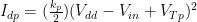
Operation Stage 4
Now, if we increase the input voltage above
For the range 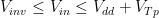
= (Vin – VTn) +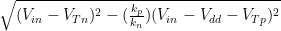
If we put 

This means that we will have the output voltage = 0 after this point.
Operation Stage 5
For the voltage range 
The PMOS is in the cut-off region, therefore the conductance of transistor M2 will be zero. This region is opposite to operation stage 1. We have the NMOS out of cut-off, but the current is zero. It means that the NMOS is in linear region with 

And also the conductivity of the NMOS transistor is given by:
 (Vin – VTn)
Shichman-Hodges Model
Recall that while both the transistors were in the saturation region at the trip point of the inverter, the output voltage varied indefinitely. This was due to the fact that we assumed the MOSFETs to be ideal current sources which they are not. So, the Schishman-Hodges Model takes into account the output resistance of the MOSFETs. In this section, we will try to come up with a value of the slope at the trip point. We will see how the slope varies w.r.t. the channel length modulation coefficient 
As there is also an output resistance present in the circuit, the current will also depend on the drain-to-source voltages for both the transistors. The schematic in figure 5 shows the DC operating point of the transistor when

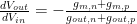
At this DC biasing point, we will perform small-signal analysis and come up with the gain of the input-output curve at this point. By shorting the large signals(as shown in figure 5 for

As we are shorting out the supply and ground, the current sources are in parallel, and also the output resistances come in parallel.
So, the conductance will add up for the output resistance in parallel. And as the small-signal gate voltage applied to the MOSFETs are the same, the transconductances will also add up for the current sources. Note that in figure 5, we already considered that with a change in small-signal voltage, the currents in NMOS and PMOS would be in opposite directions. So, placing the current sources in parallel now results in the addition of the currents flowing through the current sources.
We can write the current through the circuit to be:
 , and we also have:
 .
.
Substituting current in the above equation, we get:

This means that the gain offered by the circuit at the inversion threshold point is given by:
We replace the transconductance in the equation with:
 ;
;
 ;
;
and output conductance terms in the equations are replaced by:
 (
(
 ;
;
 ;
;
We substitute the above values in the equation for slope and finally put 

Amplification = 
Consider that we don’t have much control over the supply voltage and the threshold voltage. Then, we observe that there is only a 

Generally, we have a supply voltage 

Voltage Transfer Characteristics of CMOS
In this section, we will plot the output vs input curves that we obtained from solving the above equations. We will try to figure out the characteristics at different points of operation. Also we will plot the variation of cross-over current/drain current
Plot of output voltage vs input voltage

The “Voltage Transfer Characteristics” of the CMOS inverter is shown in figure 7. The different stages of operation of the CMOS as discussed in the mathematical derivation are also marked in the diagram.
As we can see that for 
The characteristics depend on what values of parameter we choose for the NMOS and PMOS transistors. We have seen in the derivation part that only if we choose 


Crossover current (Drain current)

The plot in figure 8 shows the drain current 
The current reaches it’s peak at region 3 which is given by a singleton point 
 ; one can also use the equation for PMOS
We know that at this point,

Substituting this value in our previous equation, we get:
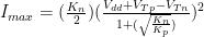
This
Inverter use in Logic gates
The performance of a digital circuit is defined by its ability to discriminate between a “High-Level” input and a “Low-Level” input. Suppose we provide an input to the inverter, which is, say close to
Similarly, we can have an input signal value close to 

The same plot for voltage transfer characteristics is plotted in figure 9. But, this time, we have drawn the figure for an understanding of the CMOS inverter from a digital circuit application point of view. There are three regions in total defined by “Logic High,” “Logic Low,” and Undefined (X). This plot will be discussed in detail when we discuss the “Noise Margins” in the next section.
Noise Margins
In the previous section, we have seen the voltage transfer characteristics of the CMOS inverter. The same plot is redrawn below for quick reference. In this section, we will analyze this curve in a detailed manner and arrive at certain conclusions from a digital circuit point of view.
For digital applications, we would like to use the CMOS inverter as a binary discriminator. This means that there will be two specific input voltages in the VTC, such that only between these two values, the inverter will amplify the signal. Outside the region defined by these two values, the inverter will attenuate the signal. These regions are marked in the plot shown in figure 10. The specific input voltages mentioned are denoted by 

In mathematical terms, attenuation means that the absolute value of gain is less than 1. Similarly, amplification means that the absolute value of the gain is more than 1. As the curve is moving from the output voltage of
The values for
The slopes can become -1 only in the regions 2 and 4. In this region, one of the transistors is in the linear region, and the other one is in the saturation region. For the ease of writing the final results, we define a quantity m as:

Then finally, solving for the values of
 –
–  ;
;
 – ;
– ;
Assuming the symmetric conditions, we get the values as:
 ,
,
 ,
,
We define the “Noise Margins” for an inverter circuit as:
Noise Margin Low = 
Noise Margin High = 
In our symmetric case, we will have

Note that the noise margins should be greater than 

For a physical implication of noise margins, one can consider that we are operating at a point such that 

But, if we do the same analysis in the region where 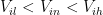
And hence the output signal for an input of
Advantages of CMOS
Before the introduction of CMOS technology, there were other logics that we used. Some of these previous technologies were RDL (Resistor Diode Logic), TTL (Transistor-Transistor Logic), ECL (Emitter Coupled Logic), NMOS (Implemented only using n-channel MOSFETs).
The CMOS technology had advantages that have made it stand out as compared to the other type of logic. Some of these advantages are mentioned below:
- Very low static power consumption
- Very small space is consumed by each logical function
- Can work with a wide range of supply voltage(3V – 15V)
- Low variation in performance with variation in temperature
- The complexity of logic gate design is reduced
Despite these advantages, the speed of TTL technology is much better than as compared to CMOS. CMOS causes more propagation delay, which is in order of 50 ns. Whereas the propagation delay for TTL is around 10 ns.
Conclusion
In this post, we have gone through the working of the simplest logic gate, the inverter. We have seen its implementation using CMOS technology. The voltage transfer characteristics is discussed in detail, along with the analytical solution for the input-output relation. We are now also familiar with the concepts of noise margins and how the CMOS inverter can be used in a digital circuit. Finally, we discussed the advantages of CMOS technology over other technologies in brief.
In the next post, we will understand the concepts regarding delays in CMOS inverters. This will give us an understanding of the speed limitations of CMOS technology. We will also see how the speed of operation varies with the power consumption in the circuit.