In the previous post, we have learned about the propagation delay in the CMOS inverter. We did a detailed derivation of the equations that quantify propagation delays for both high-to-low and low-to-high transitions. Then we have tried to understand how different parameters of the circuit affect the delay.
In this post, we will learn the power and energy consumption in a CMOS inverter. As mentioned in the earlier posts of this CMOS course, there is an inverse relationship between power consumption and the speed of the circuit. In this post, we will discuss this issue and other factors that affect the power consumption in a CMOS inverter. We will understand what “static” and “dynamic” power consumption is. For dynamic power consumption, we will derive the equations that will provide us with some design insights. Also, we will see how we quantify the figure of merit for CMOS circuits using quantities such as “Power Delay Product” and “Energy Delay Product.”
Contents
Concerns due to power consumption
Before moving forward, we should first ask ourselves why we are so concerned with power consumption in the CMOS inverter. Remember that the CMOS inverter is the fundamental building block for all our digital circuits. Some of the essential factors from an engineering point of view is that:
- Many of our circuits might have to perform using energy drawn from batteries. These stand-alone batteries can only provide a very short amount of energy. Thus, for a more extended period of operation, we would want the power consumption of our circuit to be minimum.
- In modern digital circuits, a processor can contain around a billion transistors. If each of these transistors consumes a tiny amount of power while in standby mode, even then, our total standby power consumption will be very high. Thus, if we want to make our design a scalable one, we have to ensure very low power consumption. This is infact, a prime topic in our Embedded Systems course track.
- Some of the circuits might not have any power shortage due to the easy availability of power sources. Even in such scenarios, the power consumed will result in the heating up of the components in the circuit. This will require costly heat sinks to be installed, which will only add to the cost of the overall system.
In a broad sense, there are two types of power consumption in a digital circuit. These are termed as “Static Power,” i.e., the power consumed by the circuit when it is not switching between states. And, the other one is “Dynamic Power,” i.e., the power consumed by the circuit when it is switching between states. These two powers constitute the “Total Power Dissipation” in a digital circuit. In the following sections, we have discussed these two forms of power dissipation.
Dynamic power consumption in CMOS inverter
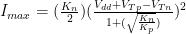
As the name suggests, dynamic power has got something to do with some changes that are occurring in the circuit. There are many nodes in the circuit that are changing from high to low voltage or low to high voltage. Let’s suppose we consider a node that corresponds to the output of a CMOS inverter gate. We will study in detail how much energy is dissipated in order to complete one full cycle of the inverter gate output. Hence, we will provide the inverter with a step pulse, as shown in figure 1.

The main factors contributing to the dynamic power dissipation are “Charging and Discharging of Load Capacitors” and “Short-Circuit Current.” We will discuss the effect of these two factors of dynamic power consumption in this section.
Charging and discharging of load capacitors
Intuitive Understanding
This is a much stronger factor than the short-circuit current, which will be discussed later. The energy dissipation for charging and discharging the load capacitor constitutes most of the dynamic energy dissipation. Now, we will see the quantitative derivation of the power dissipated in the circuit.
Suppose that initially the input is at the high-level(


We operate the digital circuits at a frequency such that each node in the overall circuit gets enough time to attain a steady-state value. Thus, before the positive edge of the input is encountered, the capacitance is charged up to the supply voltage value. Therefore, finally before to rising edge, we have 
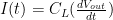
While charging the load capacitor, some of the energy is stored in the capacitor, and some energy is dissipated in the form of heat while the current flows through the resistive path provided by the PMOS. Both the energy stored in the capacitor and the energy dissipated in the PMOS transistor is supplied from the supply voltage 
Similarly, when the input encounters a positive edge, then the PMOS turns off, and the NMOS starts conducting. Thus, the charge stored in the capacitor will now get transferred to the ground via the resistive path provided by the NMOS transistor. The energy stored in the capacitor is now dissipated in the form of heat in the NMOS transistor. In the discharging cycle, there is no current drawn from the supply source. Thus there is no power consumed by the inverter during the discharge of the load capacitance. The equivalent circuit when the capacitor is discharging is shown in figure 3.

Mathematical derivation
As we previously saw that the energy is drawn from the source only during the charging of the load capacitor. We aim at figuring out the total energy drawn during the period, 

The current I(t) is the current flowing through the load capacitor, therefore:
To find the energy supplied by the source to charge the capacitor from 0 to

Here, the integral interval is from t = 0 to t = 


Therefore, the total energy supplied by the power source in the charging cycle of the load capacitor is given by:
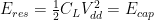
From, our knowledge of capacitors, we can say that the energy stored in a capacitor for a voltage of 


This is exactly half the energy that is supplied by the supply. Thus, we can conclude that the rest of the energy is dissipated in the resistive path offered by the PMOS transistor. One can also confirm this by doing an explicit calculation for the energy dissipated across the pull-up resistance, as shown in figure 4.
The energy that is being dissipated in the resistance is given by:

Here, voltage across the resistance = 

The discharge cycle of the capacitor can be thought of connecting the charged capacitance to the ground using a resistive path, as shown in figure 5. The NMOS transistor acts as a pull-down resistor draining the charge in the capacitance to the ground.
Thus the energy store in the capacitor(
So the total energy dissipated per cycle is given by:

Suppose, we are operating the inverter at an input frequency of 

Short-circuit current
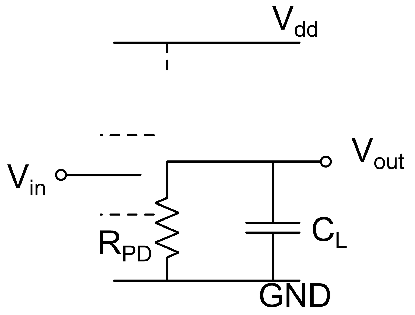
In the above cases that we have considered, the input voltage had abrupt transitions between high voltage and low voltage values. Recall that in the previous post, we have discussed the effect of a non-ideal input signal to the CMOS inverter and the delay in output pulse it causes. Similarly, in this section, we will also look at an effect that causes dynamic power dissipation due to non-ideal input voltages.
Previously, when we discussed the charging and discharging of the load capacitor, we only considered the CMOS inverter to be in stage 1 or stage 5. In both conditions, the current is equal to zero. But if we have the input signal as a ramp, then for a small amount of time, both the transistors will be “on.” This means that the NMOS and the PMOS will be drawing some current from the source and sinking it to the ground. This will result in an additional power loss in the circuit. This variation of short circuit current is shown in figure 6.
Recall that we derived the maximum drain current for an 
The current starts to rise at time t1, when 


The power dissipation due to short-circuit current is typically less than 5% of the total dynamic power dissipation. Thus, for most of the practical cases, we can neglect the power dissipation due to short-circuit current w.r.t. the power dissipation due to charging and discharging of load capacitors.
Static power dissipation
In the previous section, we have discussed the power dissipation due to the dynamic functioning of the CMOS inverter. Now, in this section, we will go over the different non-ideal cases in a CMOS inverter that causes static power dissipation. By the term “static,” we mean that the CMOS inverter output is not toggling between high and low value. The components of static power dissipation are listed below:
Gate leakage
In modern digital electronic circuits, the transistor sizes are tiny. Due to this small size, the thickness of the gate oxide layer also decreases. This results in a higher probability of gate tunneling and thus increases gate currents. These gate currents are present even when there is no transition taking place in the output voltage. Thus, it results in static power consumption.
For practical scenarios, we might have the input voltage to a circuit not being exactly equal to 0 or
Thus even in a standby mode, the CMOS inverter will provide a resistive path from the supply to the ground. The current flowing from 
Junction Leakage
The junction leakage is due to the fact that the drain terminal is in reverse bias w.r.t. the substrate. So, even in standby mode, there will be current flowing due to a formation of reverse bias in the drain-body junction. There will also be a similar effect due to “Drain Induced Barrier Lowering” (DIBL).
These non-ideal effects were discussed in an earlier post on non-ideal IV characteristics of CMOS. For a better understanding of these effects, please refer to that post.
The power dissipation due to the above mentioned non-ideal components is very low. But, suppose we are designing a processor with around a billion MOSFETs in it. The static power consumption will be present even when the inverter output is not changing between high and low. There are many inverters present in the circuit. But, all of them will not toggle for every clock pulse provided. In practical scenarios, we have circuits in which the inverters toggle once in every ten clock cycles when averaged over all the inverters in the circuit. Due to such a low rate of toggling, the static power dissipation becomes a comparable quantity to the dynamic power dissipation.
To this point, we have discussed how the power consumption in a CMOS inverter is calculated and the factors that affect it. We have seen that the dynamic energy consumed per cycle has a quadratic dependence upon the supply voltage V_{dd}. At first glance, this should suggest keeping the supply voltage V_{dd} as small as possible. But, recall that in the previous post, we have seen that the delay of a CMOS inverter is inversely proportional to the supply voltage.
This means that there is always a trade-off between the power consumed by a CMOS inverter and the maximum speed of operation it offers. Thus in order to quantify the performance of CMOS inverters, we introduce a figure of merit known as “Power-Delay Product”(PDP). In the next section, we will discuss this quantity.
Power-Delay Product
We have seen that for a given CMOS inverter, the average power consumed is given by:
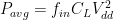
And, suppose the propagation delay for rising and falling is same, i.e. 


Therefore, the power delay product of the CMOS inverter is defined as:
PDP = 
From this equation, we can understand that as the PDP increases, the inverse relation between dynamic power consumption and delay of the inverter becomes stronger. Suppose, we want to decrease our delay of the circuit for some particular application. If the PDP has a very high value, then the decrease in delay will have to be compensated by a large increase in power consumption. But, if we have a CMOS inverter with a very low PDP, then we can decrease the delay with a much lower rise in power consumption.
Another thing to notice in the equation is that the PDP has a quadratic dependence on the load capacitance 
The PDP is dependent on the input frequency
Energy-Delay Product
Similar to the power delay product, the Energy delay product is given by the product of delay, and the energy dissipated in the circuit per cycle. The equation for EDP is similar to that of PDP; the only difference is the absence of the input frequency term
EDP = 
Recall that we generally operate at a frequency which is about 20 times less than the maximum frequency of operation of a CMOS inverter. Thus, we typically have:

In the calculation of PDP, there is a large factor (around 40) in the denominator. So we can still have an inferior performance for certain circuits with low PDP.
Thus the “energy-delay product” is a much better figure of merit when we are comparing different digital circuits or different logic families.
Conclusion
In this post, we have seen the static and dynamic power consumption in a CMOS inverter. We have derived the formula for average dynamic power consumption(
In the next post, we will move on to the design of different logic gates using CMOS inverters. We will see how the understanding we have developed for the CMOS inverter will help in coming up with circuits for digital logic gates. The delay, power, and noise parameters discussed for the CMOS inverter are very important for further understanding of digital logic design. The CMOS inverter will be the fundamental building block of digital circuits that we discuss later in this course. Thus a firm understanding of CMOS inverter is fundamental.